MARVEL Series Laser Cutting Machine
SMART Series Laser Cutting Machine

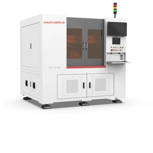
Suitable for laser cutting of alumina, zirconium oxide, aluminum nitride, silicon nitride and other ceramic materials, equipped with loading and unloading mechanism to achieve high efficiency and high precision automatic processing.
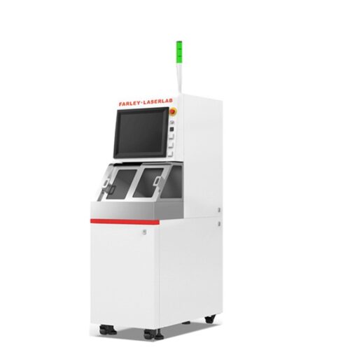
This equipment is mainly developed for semiconductor and 3C industries. Suitable for cutting silicon, ceramics, glass, SiC and other materials. It has the advantages of fast cutting speed and high positioning accuracy. The equipment is equipped with a high-precision CCD vision system
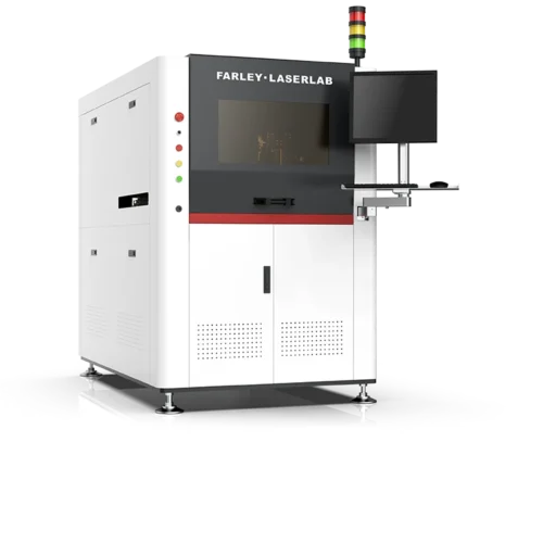
FPC laser cutting machines adopt high-performance cold laser source, perfectly achieving the board shape cutting, contour cutting, drilling and cover film cutting and other ultra-fine processing. The equipment is mainly used in precision cutting and marking for flexible circuit boards, rigid circuit boards, rigid-flexible circuit boards.
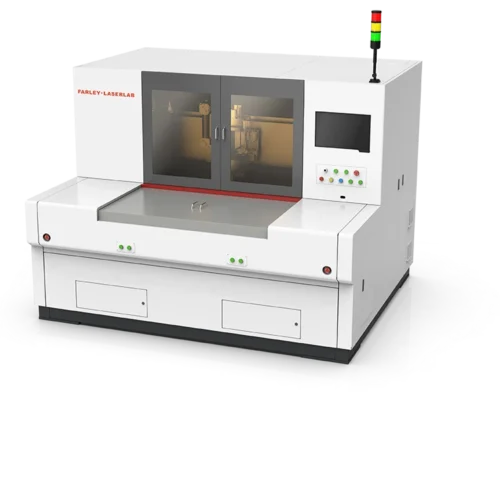
Mainly used for FPC covering film cutting, FPC shape cutting, FPC window half cutting and RFPC cover opening etc. It has high accuracy, high stability and consistent cutting HAZ effect.
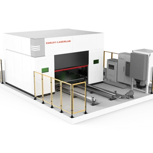
In fact, in China, the first three laser cutting equipment were all from our company, which provides durable services to all customers. After decades of efforts, we have won 5 innovations, 7 surpass, 26 invention patents, 39 utility models and 2 software
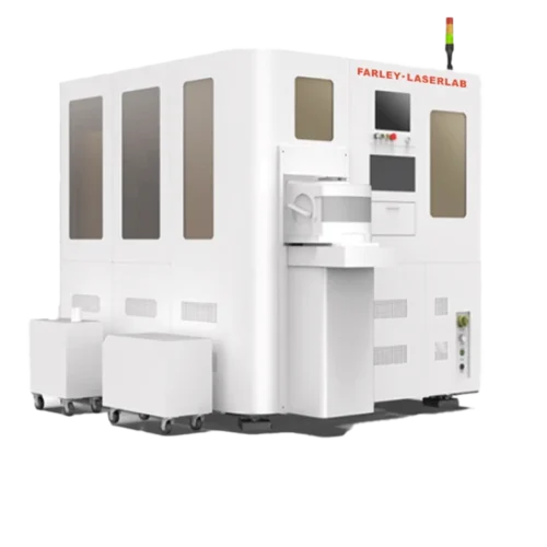
For the pan semiconductor and 3C industries, it is applied to various types of identification of Si, Gan, SiC, glass and surface coating materials, and is applicable to 8-inch and above wafers.
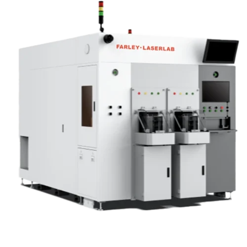
FARLEY·LASERLAB LUA3200 Ultra-efficient Fully Automated Wafer Laser Annealing Machine:The EFEM system pre-positions the wafer, a customized laser annealing head and precision motion platform work together to anneal the entire SiC wafer backside metal (Ni or T layer), ensuring good ohmic contact,
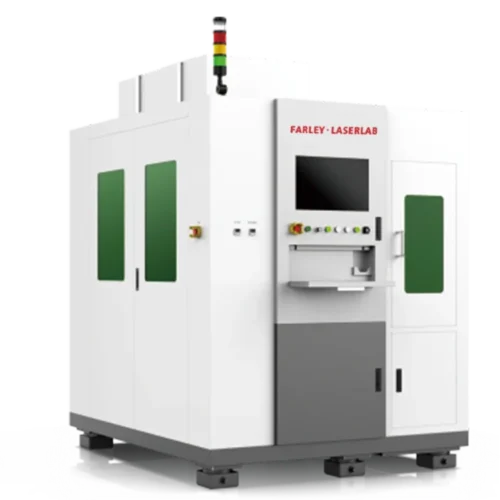
SiC wafer laser hidden cutting equipment, internal modification to form a crack layer, no tool loss, no frontal damage, suitable for the mass production of vehicle-grade SiC chips.
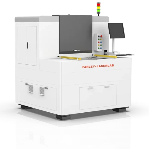
Developed for high-speed, high-precision drilling applications for soft and rigid combination boards and other materials, with high precision, high efficiency, micro-hole processing, and convenient shape change, as well as processing for shape and cover film cutting.
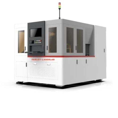
Used for automatic identification and laser marking scrap unit on carrier products, which facilitates efficient and accurate identification of subsequent processes and improves the product yield and process efficiency of customer factories.With the development of printed circuit boards towards refinement
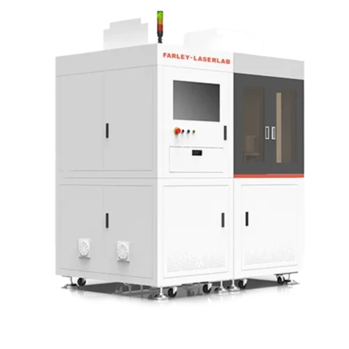
Facing the upstream raw material manufacturing enterprises and the midstream wafer manufacturing enterprises in the semiconductor industry chain, the independent developed optical bright and dark field detection system is used to detect the appearance defects of semiconductor raw materials, epitaxial wafers and patterned wafers.
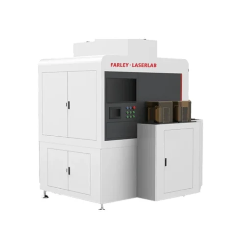
For the mid stream wafer manufacturing enterprises and downstream packaging and testing enterprises in the semiconductor industry chain, a multi-channel bright and dark field parallel detection system developed independently is