MARVEL Series Laser Cutting Machine
SMART Series Laser Cutting Machine

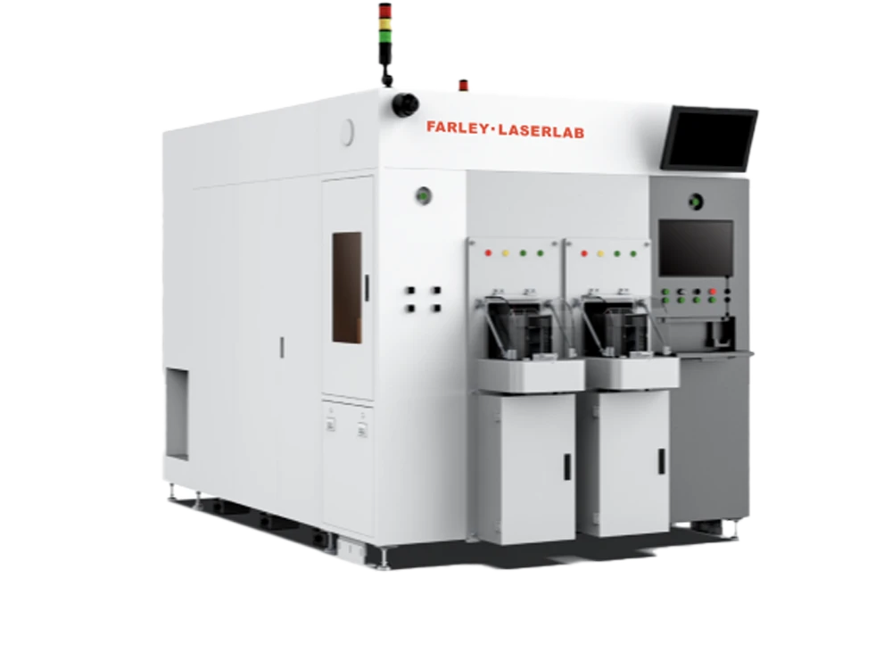
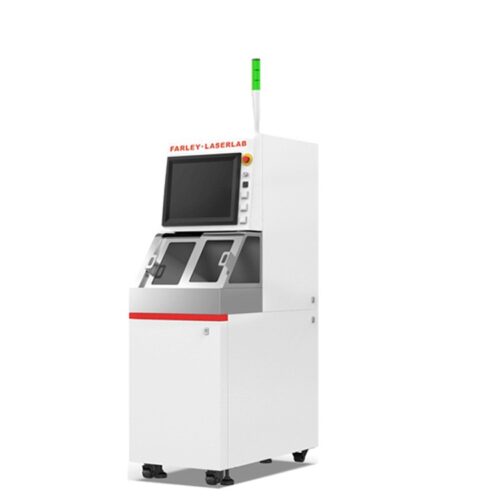
FARLEY·LASERLAB LUA3200 Ultra-efficient Fully Automated Wafer Laser Annealing Machine:The EFEM system pre-positions the wafer, a customized laser annealing head and precision motion platform work together to anneal the entire SiC wafer backside metal (Ni or T layer), ensuring good ohmic contact,
FARLEY·LASERLAB LUA3200 Ultra-efficient Fully Automated Wafer Laser Annealing Machine:The EFEM system pre-positions the wafer, a customized laser annealing head and precision motion platform work together to anneal the entire SiC wafer backside metal (Ni or T layer), ensuring good ohmic contact, reduced contact resistance, and improved device performance.
This FARLEY·LASERLAB LUA3200 wafer laser annealing machine uses EFEM system and precision laser module to perform full backside annealing for SiC wafers, lowering contact resistance with low carbon deposition and low surface temperature, and fully meeting SEMI semiconductor standards.
SEMI certified for the semiconductor industry
Ultra-low contact resistivity
Low surface temperature annealing
Contact resistivity < 10-5 Ω·cm² after annealing.
Low carbon deposition performance
With a semiconductor-standard EFEM front-end system
EFEM system pre-positions wafers; customized laser head and precision platform perform full SiC wafer backside metal annealing.
Ensures excellent ohmic contact, reduces contact resistance, and effectively improves overall device performance.Low carbon deposition,non-annealed surface temperature <120°C.Certified by SEMI Semiconductor Industry Standards.

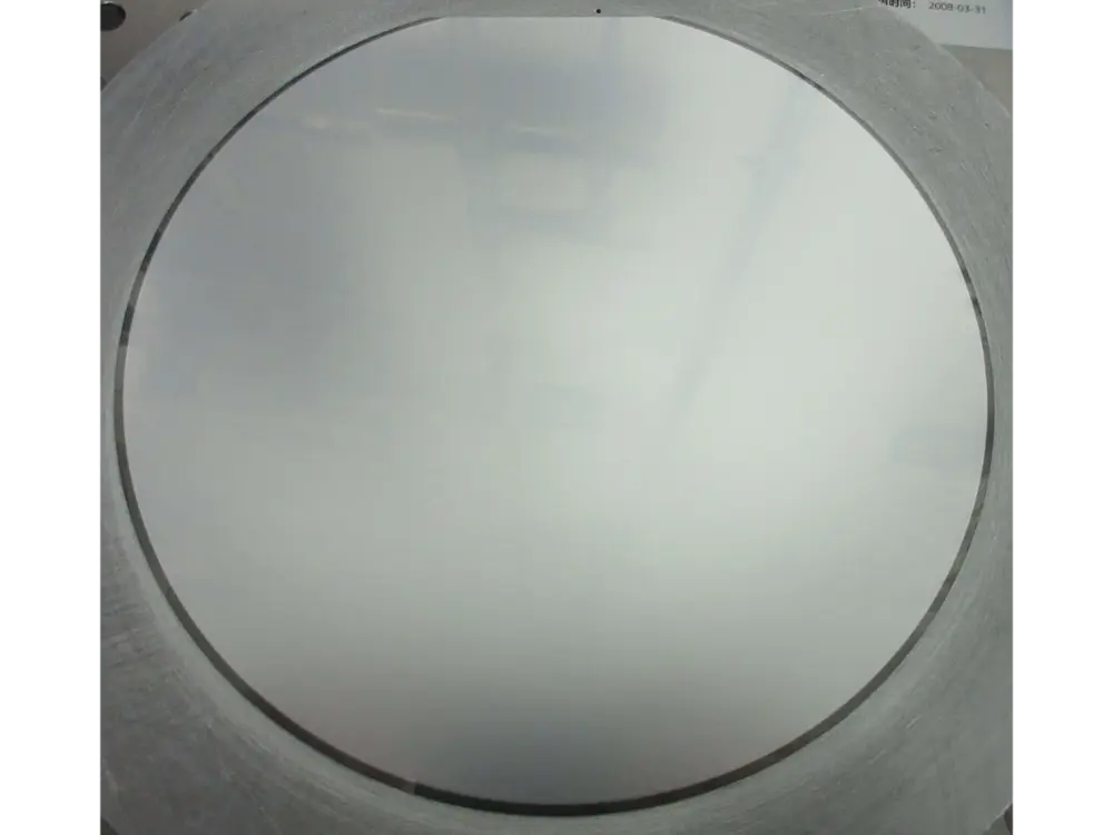

This equipment is mainly developed for semiconductor and 3C industries. Suitable for cutting silicon, ceramics, glass, SiC and other materials. It has the advantages of fast cutting speed and high positioning accuracy. The equipment is equipped with a high-precision CCD vision system
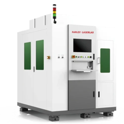
SiC wafer laser hidden cutting equipment, internal modification to form a crack layer, no tool loss, no frontal damage, suitable for the mass production of vehicle-grade SiC chips.
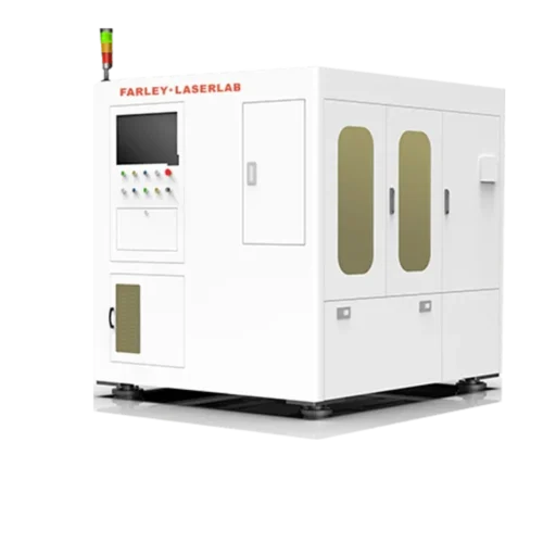
This equipment is used for laser modification and cutting of silicon-based wafers in the semiconductor industry for 8-inch and above chip sealing and testing plants.
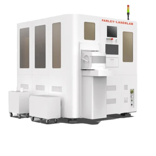
For the pan semiconductor and 3C industries, it is applied to various types of identification of Si, Gan, SiC, glass and surface coating materials, and is applicable to 8-inch and above wafers.