MARVEL Series Laser Cutting Machine
SMART Series Laser Cutting Machine

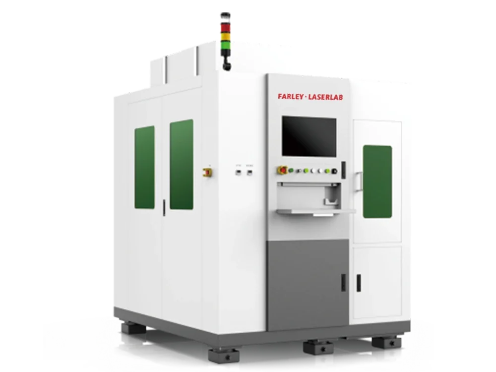
SiC wafer laser hidden cutting equipment, internal modification to form a crack layer, no tool loss, no frontal damage, suitable for the mass production of vehicle-grade SiC chips.
SiC wafer laser hidden cutting equipment, internal modification to form a crack layer, no tool loss, no frontal damage, suitable for the mass production of vehicle-grade SiC chips.
This LUSD3310 fully automatic equipment processes 6–8 inch SiC wafers via CCD vision positioning and ultrafast laser stealth dicing. With dynamic focus compensation, enclosed optical path and self-developed software, it delivers ≤±3μm precision, complies with SEMI standards, and supports customized processing for various wafers.
Auto CCD vision positioning
Dynamic focus compensation
SEMI industry compliant
Ultrafast laser stealth dicing
≤±3μm high precision
Customizable software modules
Through the self-developed dynamic focus compensation module, with the high-precision air flotation linear motion platform, high-precision and high-consistency wafer processing can be realized, and the processing quality reaches the leading level in the industry.
Configure the standard design of the implicit outer optical path black box, stable transmission of laser beam, stable output of laser energy, good processing stability
Independently develop cutting and vision software, provide customized functional modules, with a high degree of customization, meet the needs of the industry
| Project | Main technical parameters | |
|---|---|---|
| Main parameters | Equipment model | LUSD 3310 |
| Laser light source | Infrared | |
| loading and unloading method | Fully automatic, CST to CST | |
| Processing performance | Processing materials | 6/8inch SiC |
| Processing accuracy | ≤±3μm | |
| Processing speed | ≥500mm/s | |
Certified by SEMI Semiconductor Industry Standards.
Integrated with high-precision Dynamic Focus Compensation System (DFT) and Autofocus System
Customizable vision and cutting software modules adaptable to various wafer types.
Achieves processing precision of ≤ ±3 microns, meeting advanced industry benchmarks; supports 6-8 inch wafers with dynamic focus compensation, autofocus, and auto-alignment to meet diverse processing needs.
Equipped with SEMI-standard automated wafer handling and inspection systems.

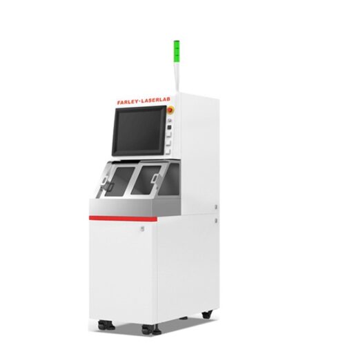
This equipment is mainly developed for semiconductor and 3C industries. Suitable for cutting silicon, ceramics, glass, SiC and other materials. It has the advantages of fast cutting speed and high positioning accuracy. The equipment is equipped with a high-precision CCD vision system
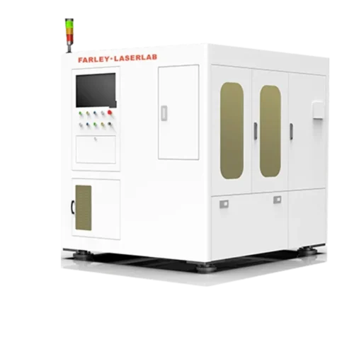
This equipment is used for laser modification and cutting of silicon-based wafers in the semiconductor industry for 8-inch and above chip sealing and testing plants.
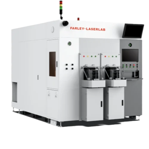
FARLEY·LASERLAB LUA3200 Ultra-efficient Fully Automated Wafer Laser Annealing Machine:The EFEM system pre-positions the wafer, a customized laser annealing head and precision motion platform work together to anneal the entire SiC wafer backside metal (Ni or T layer), ensuring good ohmic contact,
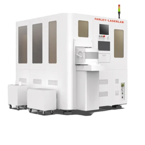
For the pan semiconductor and 3C industries, it is applied to various types of identification of Si, Gan, SiC, glass and surface coating materials, and is applicable to 8-inch and above wafers.