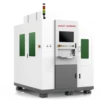
MARVEL Series Laser Cutting Machine
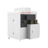
SMART Series Laser Cutting Machine

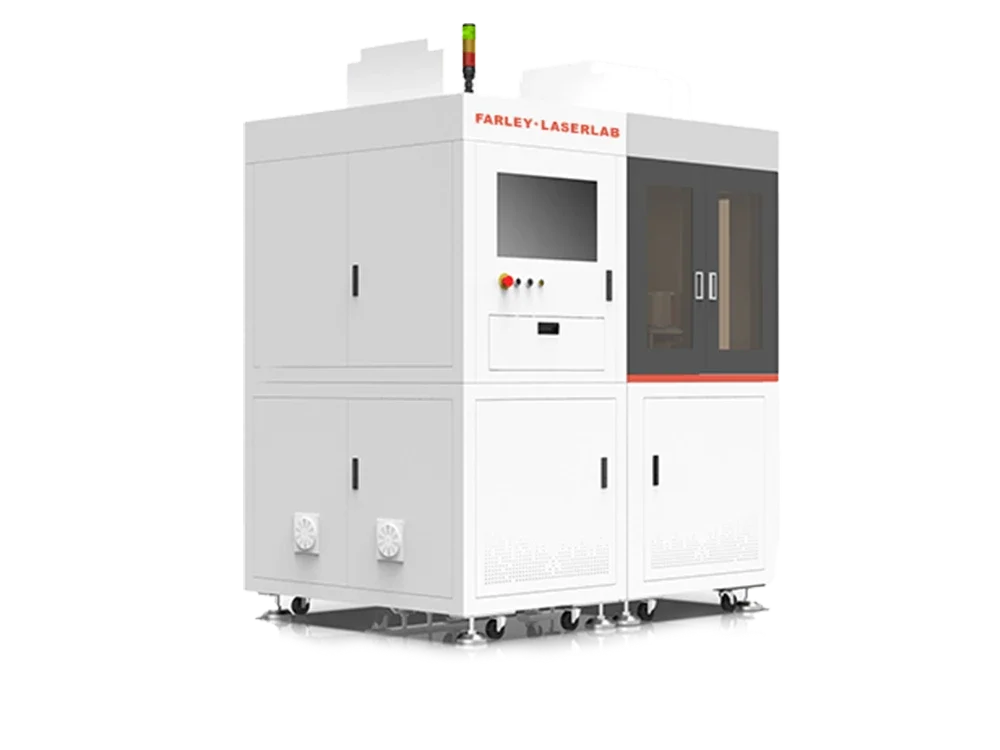
Facing the upstream raw material manufacturing enterprises and the midstream wafer manufacturing enterprises in the semiconductor industry chain, the independent developed optical bright and dark field detection system is used to detect the appearance defects of semiconductor raw materials, epitaxial wafers and patterned wafers.
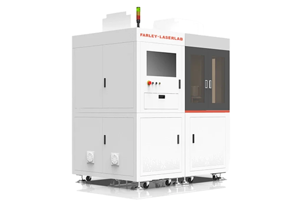
This wafer inspection machine suits 4–8 inch various wafers, detects multiple surface defects with 1–10μm high resolution and fast speed, serving semiconductor raw material and wafer manufacturers.
Compatible with 4–8 inch various wafers
1–10μm high resolution
Bright & dark field optical system
Detects multiple surface defects
Fast wafer inspection speed
For semiconductor wafer manufacturing
| Item | Main parameters | |
|---|---|---|
| General parameters | Wafer size | Standard 4 “, 6” (expandable 4 “- 8”) |
| Number of boxes | Double-deck, 14 pcs | |
| Loading and unloading method | Robot, mapping scanning | |
| Motion platform | Y stroke 350mm,repetitive accuracy 10μm Z strooke 8mm,repetitive accuracy 5μm | |
| Capacity | 4″ , 140WPH 6″ , 120WPH | |
| Detection performance | Test accuracy | 7 μm |
| Camera | High resolution industrial camera | |
| Lens | HD industrial lens | |
| Light source | Patented light source | |
| Environment requirement | Power supply specification | AC220V, 50Hz |
| Air source requirements | 0 .5-0 .7Mpa compressed air, without obvious water vapor and grease | |
| Using environment | Temperature: 15-40 ℃. Humidity requirement: 30% – 70%, no frost | |
| Overall size | 1800mm*1300mm*2250mm | |
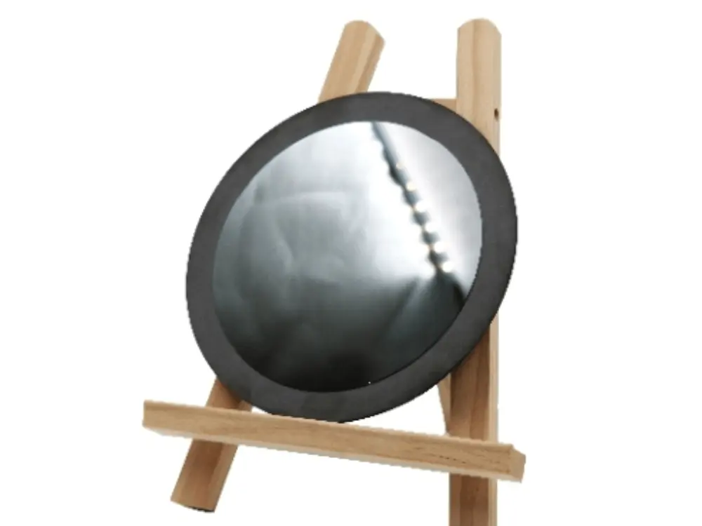
Suitable for 4-8 inch wafers, substrates, epitaxial wafers and patterned wafers.
Detect particles, pits, bumps, scratches, stains, cracks and other defects.
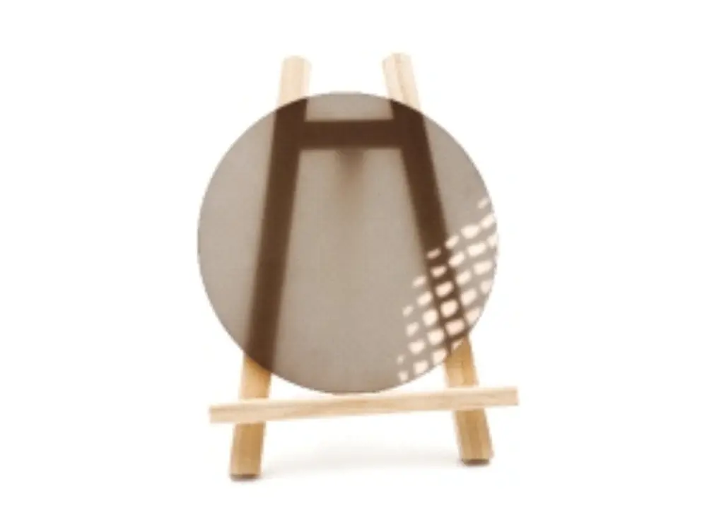
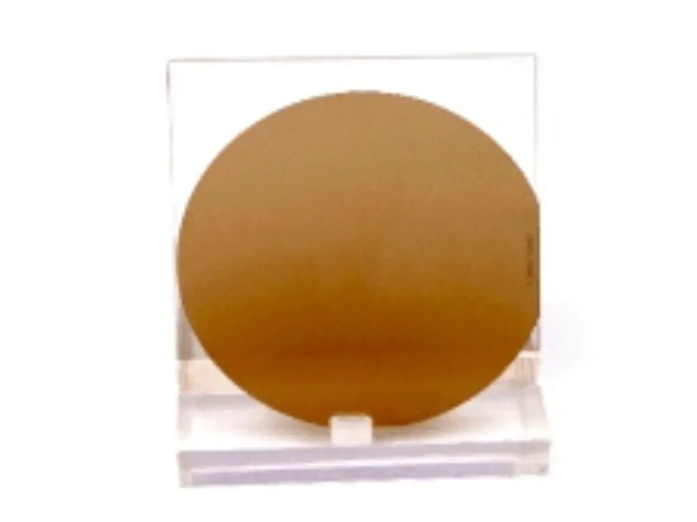
System resolution: 1-10 μ m.
No pattern wafer: 180 seconds / wafer when the number of defects is less than 200.
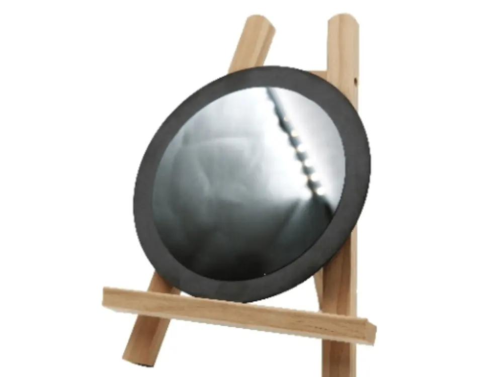
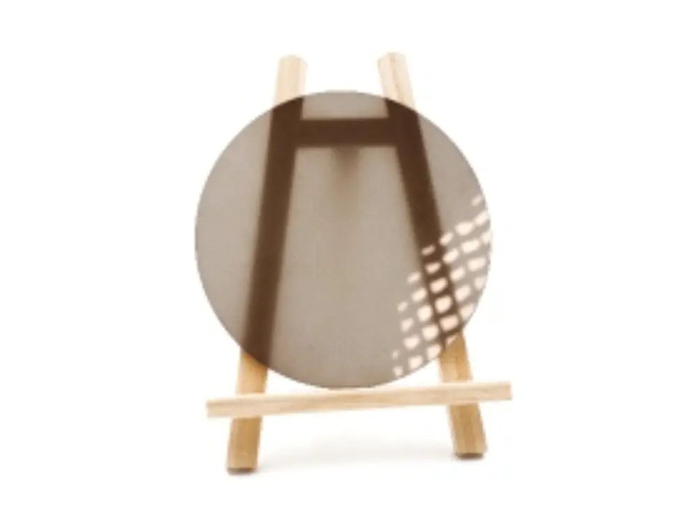
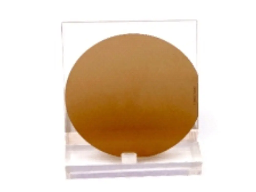
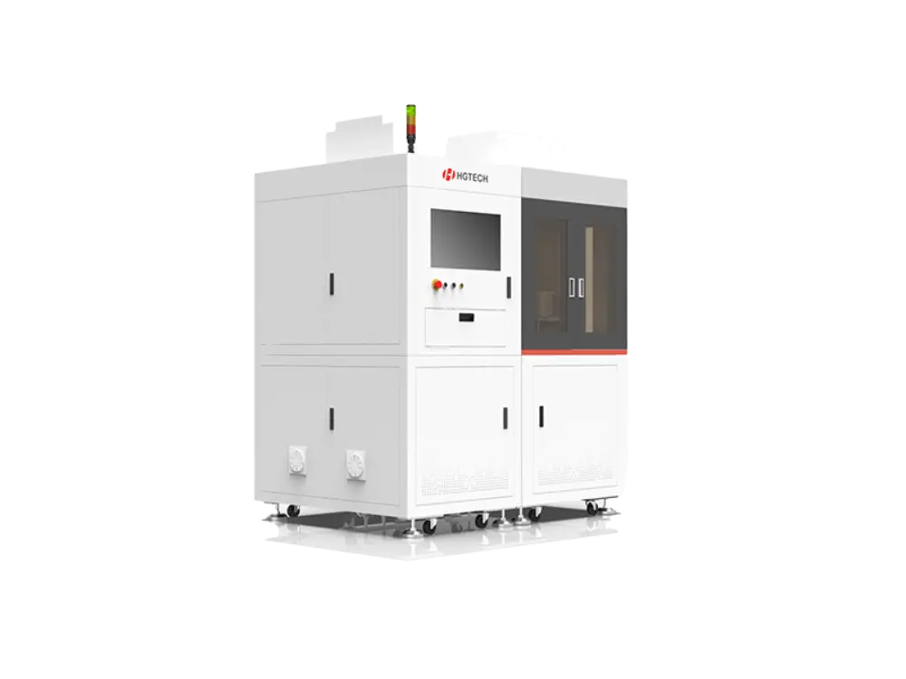

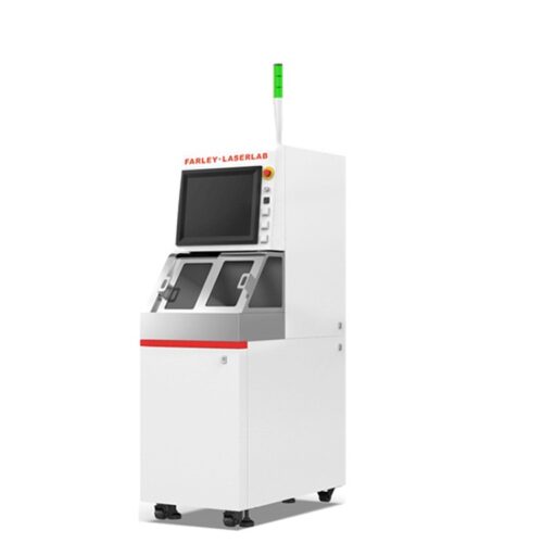
This equipment is mainly developed for semiconductor and 3C industries. Suitable for cutting silicon, ceramics, glass, SiC and other materials. It has the advantages of fast cutting speed and high positioning accuracy. The equipment is equipped with a high-precision CCD vision system
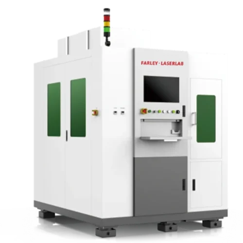
SiC wafer laser hidden cutting equipment, internal modification to form a crack layer, no tool loss, no frontal damage, suitable for the mass production of vehicle-grade SiC chips.
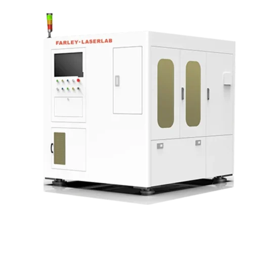
This equipment is used for laser modification and cutting of silicon-based wafers in the semiconductor industry for 8-inch and above chip sealing and testing plants.
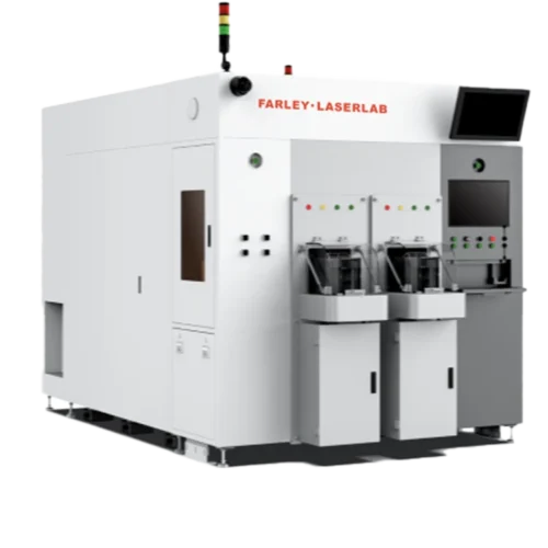
FARLEY·LASERLAB LUA3200 Ultra-efficient Fully Automated Wafer Laser Annealing Machine:The EFEM system pre-positions the wafer, a customized laser annealing head and precision motion platform work together to anneal the entire SiC wafer backside metal (Ni or T layer), ensuring good ohmic contact,