MARVEL Series Laser Cutting Machine
SMART Series Laser Cutting Machine

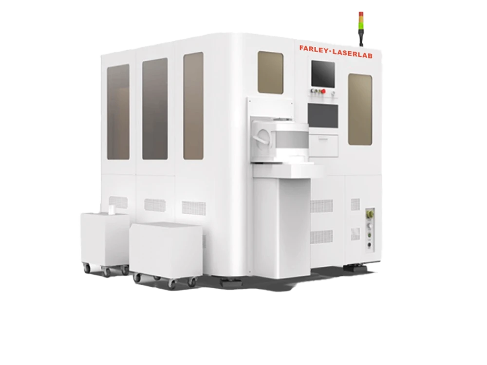
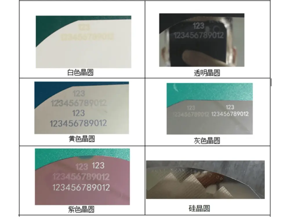
For the pan semiconductor and 3C industries, it is applied to various types of identification of Si, Gan, SiC, glass and surface coating materials, and is applicable to 8-inch and above wafers.
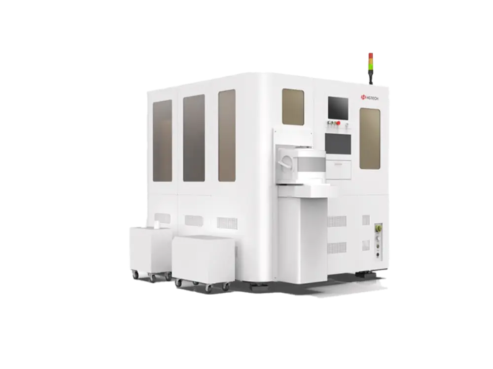
This picosecond laser marking machine features low thermal impact and supports multiple code formats. It enables MES data uploading, fits 8–12 inch wafers with full auto loading/unloading, and adopts a marble base for stable performance, ideal for semiconductor and 3C material marking.
Picosecond laser, low thermal impact
MES system data uploadable
Full auto loading & unloading
Multi-format marking supported
Compatible with 8–12 inch wafers
Marble base for high stability
| HD S2113 | Main parameters | |
|---|---|---|
| Laser | Average output power | ≥5W(optional) |
| Pulse width | <10ps | |
| Laser wavelength | Lamp Source | |
| Linear motor parameters CCD positioning system Code reading system | Motor stroke | 450*650mm |
| Pixel | 12 million pixels, positioning accuracy 0.003mm | |
| Pixel | 600 million pixels | |
| Machining accuracy | Positioning accuracy | ≤±0.03mm |
| Machining dimensional accuracy | ≤±0.02mm | |
| Handling robot | Number of robot arms | Single / double arm |
| Finger | Clamping / adsorption | |
| Others | Charging machine | Yes |
| Mapping | Yes | |
| Edge finder | 8- 12inch is compatible | |
| General indicators | Cleanliness level | Hundred level 500 |
| Size | 1900mm*1800mm*1950mm(main body) | |
| Weight | About 2.5t | |
Equipped with code reading module to support information uploading to MES system.
The equipment is compatible with 8-12inch wafers, fully automatic loading and unloading.
Equipped with load mechanism, which can automatically open / close the wafer cassette.
Marble base, stable optical path system, thus ensuring high-quality optical transmission.
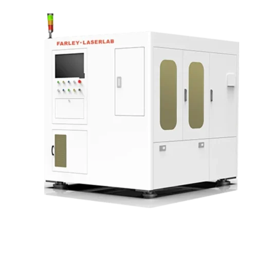
This equipment is used for laser modification and cutting of silicon-based wafers in the semiconductor industry for 8-inch and above chip sealing and testing plants.
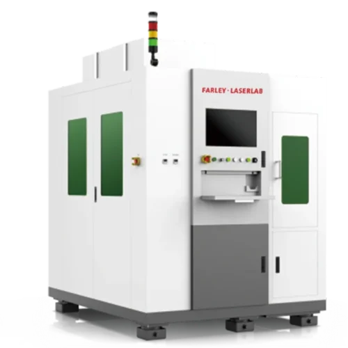
SiC wafer laser hidden cutting equipment, internal modification to form a crack layer, no tool loss, no frontal damage, suitable for the mass production of vehicle-grade SiC chips.
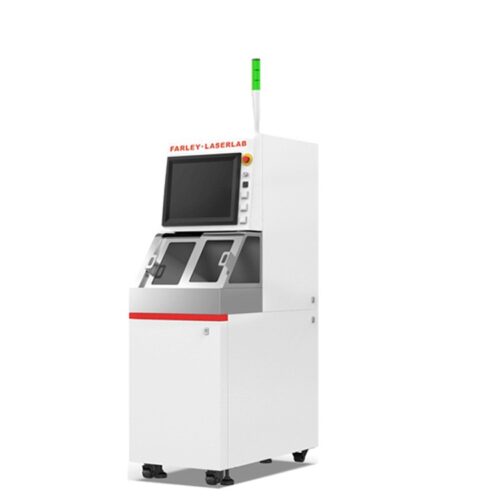
This equipment is mainly developed for semiconductor and 3C industries. Suitable for cutting silicon, ceramics, glass, SiC and other materials. It has the advantages of fast cutting speed and high positioning accuracy. The equipment is equipped with a high-precision CCD vision system
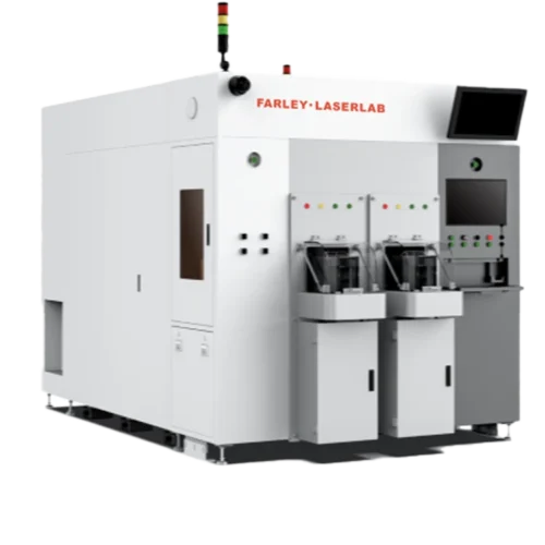
FARLEY·LASERLAB LUA3200 Ultra-efficient Fully Automated Wafer Laser Annealing Machine:The EFEM system pre-positions the wafer, a customized laser annealing head and precision motion platform work together to anneal the entire SiC wafer backside metal (Ni or T layer), ensuring good ohmic contact,