MARVEL Series Laser Cutting Machine
SMART Series Laser Cutting Machine

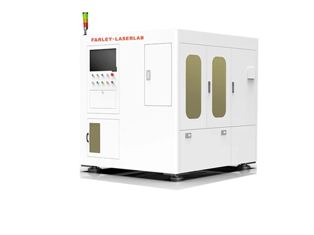
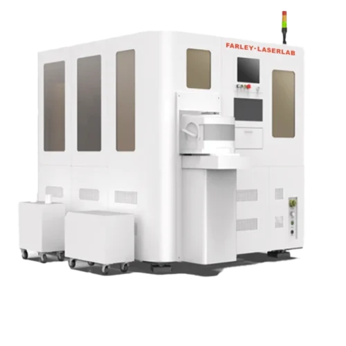
This equipment is used for laser modification and cutting of silicon-based wafers in the semiconductor industry for 8-inch and above chip sealing and testing plants.
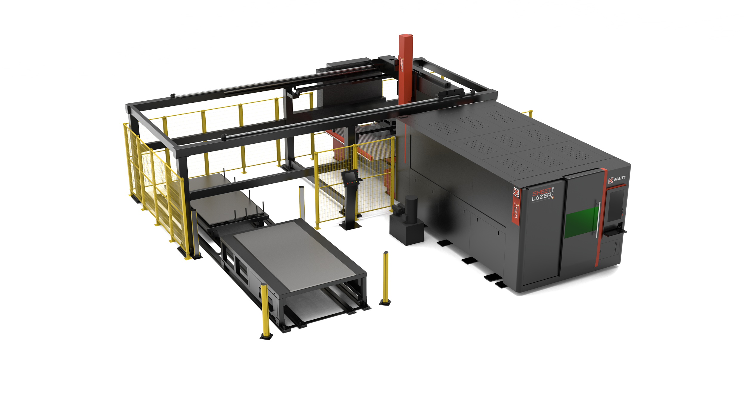
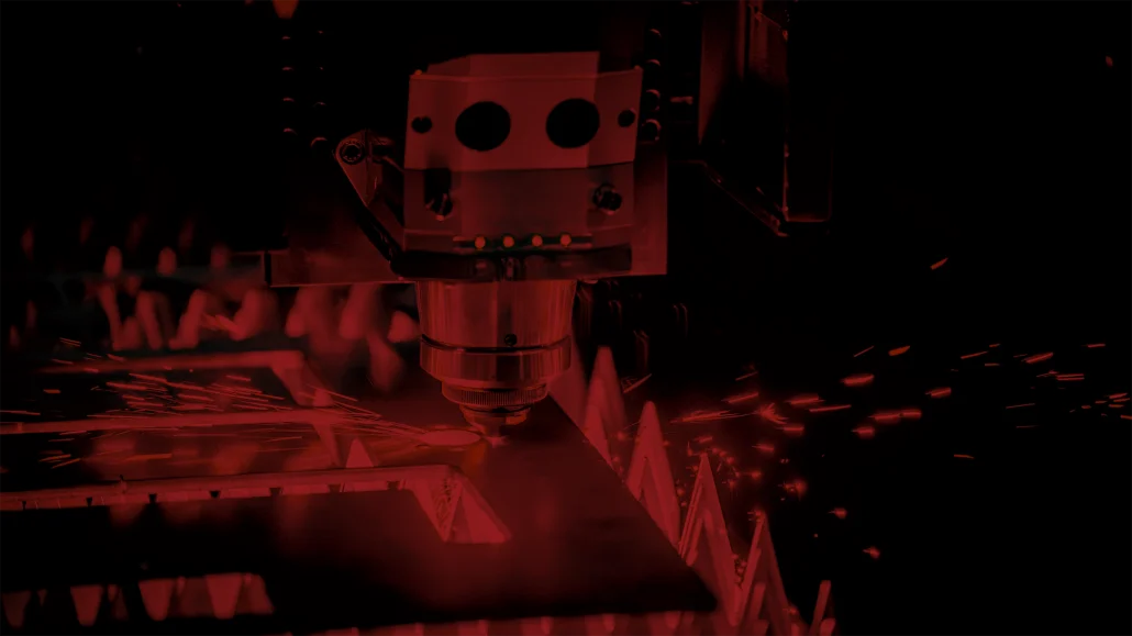
This equipment is used for laser modification and cutting of silicon-based wafers in the semiconductor industry for 8-inch and above chip sealing and testing plants.
This equipment performs laser modification and cutting for 8-inch+ silicon-based wafers, featuring ultra-small edge collapse, multi-focus high efficiency and stable laser output.
http://无
Zero surface damage
Smooth edge < 3μm
Laser power stability ≤±3%
Edge collapse ≤ 2μm
Multi-focus high efficiency
High beam quality M²<1.5
6/12inch silicon wafer laser modification hidden cutting equipment, internal modification without mechanical damage, narrow wafer design to improve wafer utilization rate, suitable for ultra-thin wafer processing.
| Item | Main parametetrs | |
|---|---|---|
| Laser | Center wavelength | Custom infrared wavelength |
| Cutting head | Self-developed collimating head | |
| Performance | Effective working stroke | 300x400mm(optional) |
| Repetitive positioning accuracy | ±1μm | |
| Visual positioning | Automatic visual positioning | |
| Processing method | Layer by layer upgrading, single point / multi-point processing | |
| Others | Wafer size | 8 inch (12inch is compatible ) |
| Processing process | Laser modified cutting – film spreading | |
| Processing object | MEMS chip, silicon-based biochip, silicon wheat chip, CMOS chip, etc | |
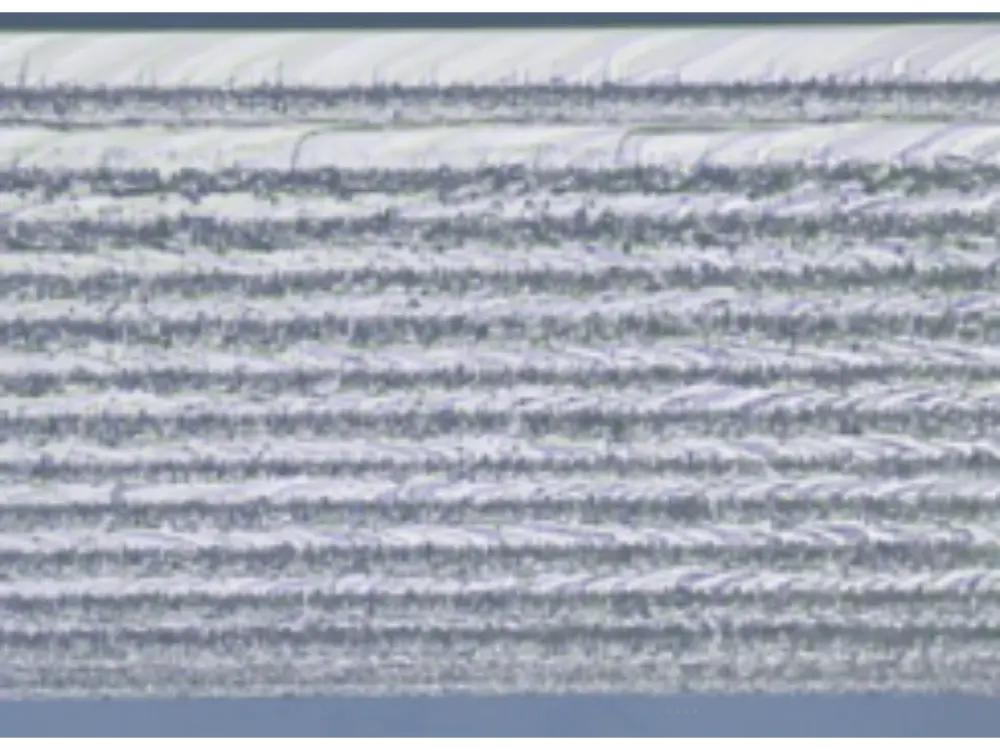
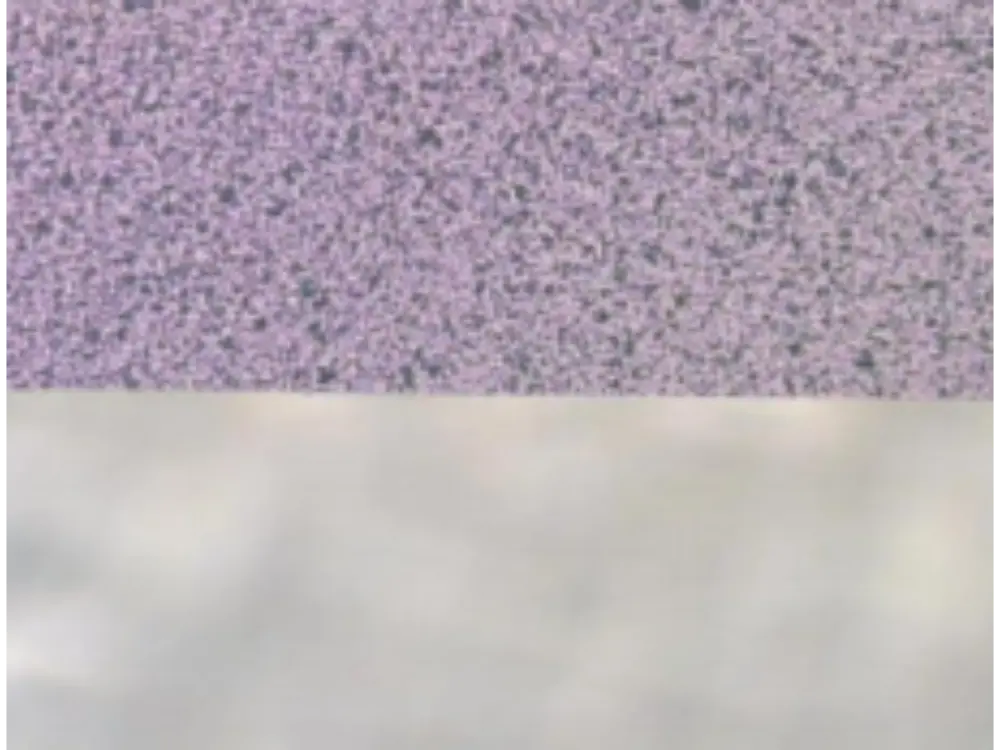
8 inch silicon-based wafer, single point layer by layer modification, thickness 730 μ m.
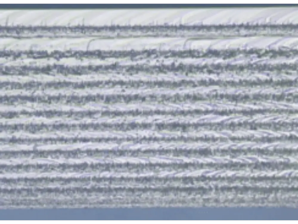

8 inch silicon-based wafer, single point layer by layer modification, thickness 730 μ m.
8 inch silicon-based wafer, single point layer by layer modification, thickness 730 μ m.
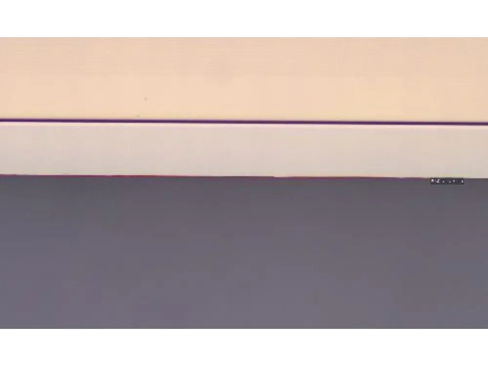


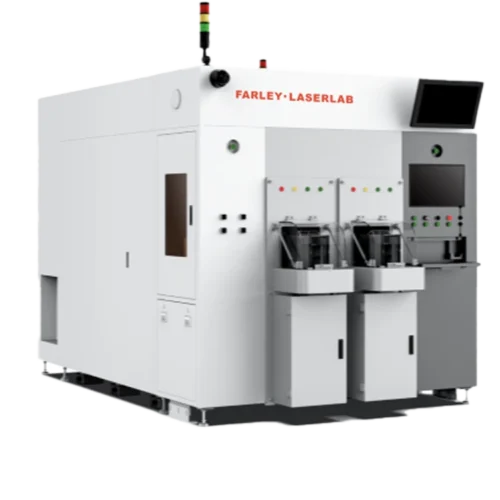
FARLEY·LASERLAB LUA3200 Ultra-efficient Fully Automated Wafer Laser Annealing Machine:The EFEM system pre-positions the wafer, a customized laser annealing head and precision motion platform work together to anneal the entire SiC wafer backside metal (Ni or T layer), ensuring good ohmic contact,
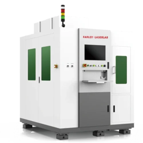
SiC wafer laser hidden cutting equipment, internal modification to form a crack layer, no tool loss, no frontal damage, suitable for the mass production of vehicle-grade SiC chips.
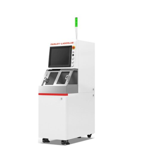
This equipment is mainly developed for semiconductor and 3C industries. Suitable for cutting silicon, ceramics, glass, SiC and other materials. It has the advantages of fast cutting speed and high positioning accuracy. The equipment is equipped with a high-precision CCD vision system
For the pan semiconductor and 3C industries, it is applied to various types of identification of Si, Gan, SiC, glass and surface coating materials, and is applicable to 8-inch and above wafers.