MARVEL Series Laser Cutting Machine
SMART Series Laser Cutting Machine

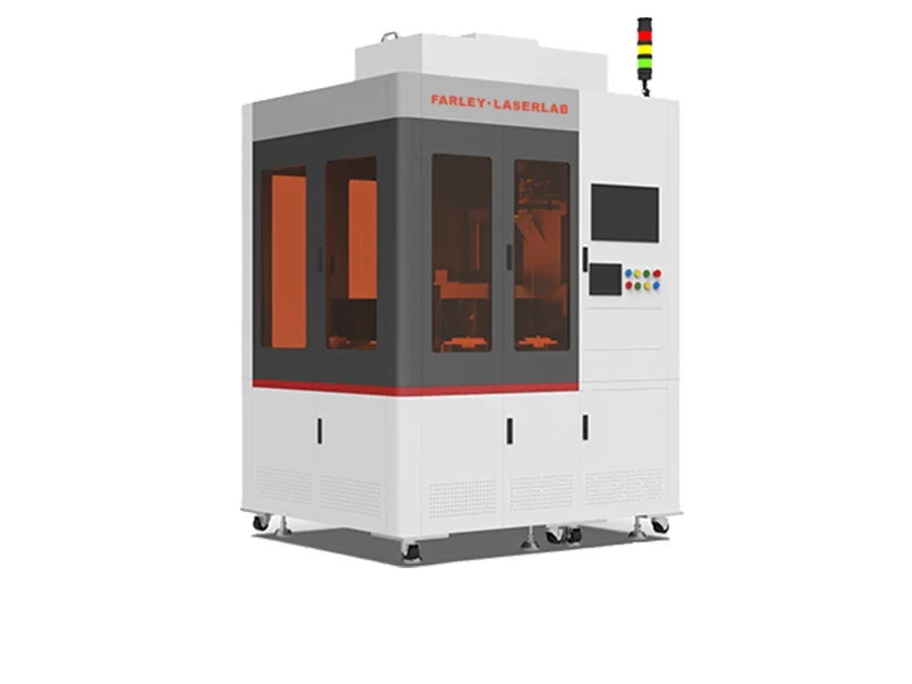
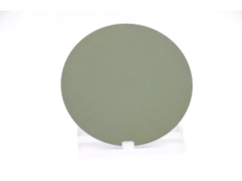
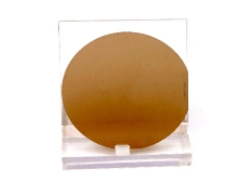
Facing the raw material production enterprises in the upstream of the semiconductor industry chain, the independently developed spectral confocal measurement system is used to detect the size and flatness of semiconductor raw and epitaxial wafers.

This spectral confocal measuring device is for 4–8 inch raw, substrate and epitaxial wafers. It delivers ±1μm high accuracy with fast 30s per piece testing, ideal for semiconductor raw material manufacturers.
Fits 4–8 inch various wafers
±1μm high thickness accuracy
Fast 30s per wafer measurement
Spectral confocal measurement system
0.2μm excellent repeatability
Wafer size and flatness inspection
| Item | Main parameters | ||
|---|---|---|---|
| General parameters | Wafer size | 4″ , 6″ | |
| Number of boxes | Double-deck, 14 pcs | ||
| Loading and unloading method | Robot, mapping scanning | ||
| Motion platform | X stroke150mm, Y stroke150mm, | Repetitive accuracy ±0. 1 μm Repetitive accuracy ±0. 1 μm | |
| Capacity | 4″ , 240WPH 6″ , 220WPH | ||
| Detection performance | Detection function | Wafer (coated wafer) thickness, TTV, warpage | |
| Thickness test accuracy | ±0 .5 μ m. Repeatability: 0.1 μ M (25 pieces continuously tested, 5 points for each piece) | ||
| Thickness range | ± 1 mm | ||
| TTV test accuracy | ± 0.5 um, repeatability: 0.2 μ m | ||
| Warpage test accuracy | ± 2 μ m. Test range: ± 600 μ m. Repeatability: 1 μ m | ||
| Environment requirement | Power supply specification | AC220V,50Hz | |
| Air source requirements | 0.5-0.7mpa compressed air, without obvious water vapor and grease | ||
| Using environment | Temperature: 15-40 ℃. Humidity requirement: 30% – 70%, no frost | ||
| Overall size | 1800mm*1300mm*2250mm | ||
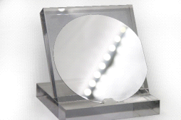
Used for 4-8 inch original wafer, substrate and epitaxial wafer of various materials and polishing conditions.
Thickness range: 0-1mm measurement accuracy: ± 1 μ M repetition accuracy: 0.2 μ m.
Measurement time: 30s / PCS (according to the customer’s detection trajectory).
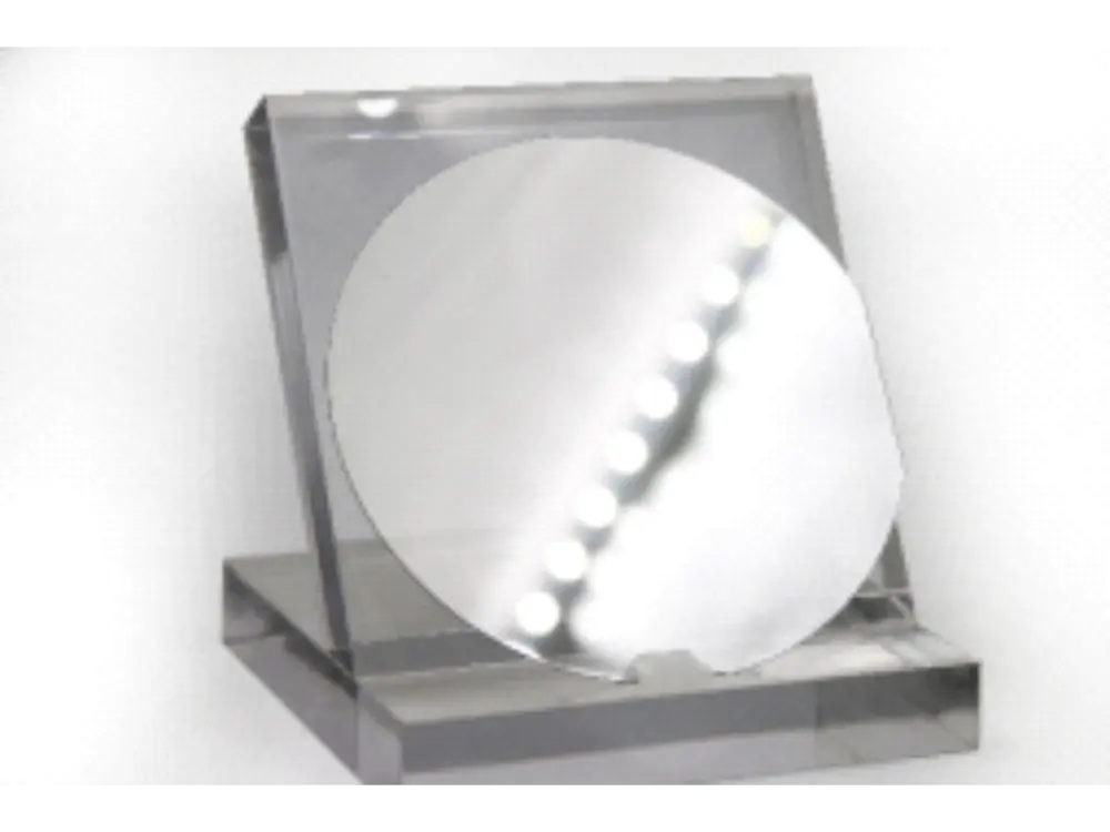

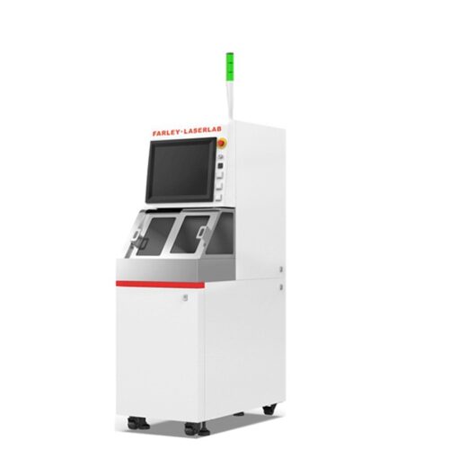
This equipment is mainly developed for semiconductor and 3C industries. Suitable for cutting silicon, ceramics, glass, SiC and other materials. It has the advantages of fast cutting speed and high positioning accuracy. The equipment is equipped with a high-precision CCD vision system
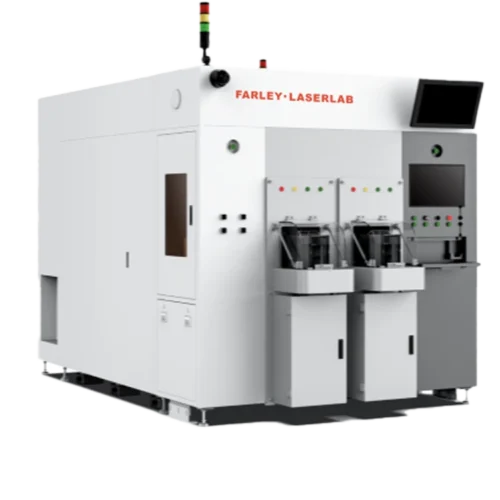
FARLEY·LASERLAB LUA3200 Ultra-efficient Fully Automated Wafer Laser Annealing Machine:The EFEM system pre-positions the wafer, a customized laser annealing head and precision motion platform work together to anneal the entire SiC wafer backside metal (Ni or T layer), ensuring good ohmic contact,
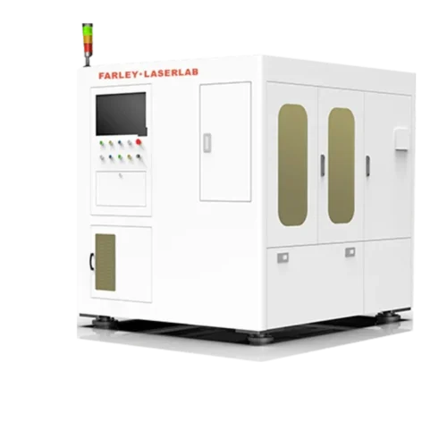
This equipment is used for laser modification and cutting of silicon-based wafers in the semiconductor industry for 8-inch and above chip sealing and testing plants.
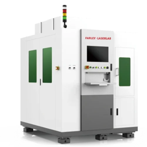
SiC wafer laser hidden cutting equipment, internal modification to form a crack layer, no tool loss, no frontal damage, suitable for the mass production of vehicle-grade SiC chips.